The IIS Chip Gallery
Flintstone (1986)

Additional pictures below, click to see larger versions


by


| Application | Processor |
| Technology | 2000 |
| Manufacturer | Faselec |
| Type | Research |
| Package | PGA84 |
| Dimensions | 6200μm x 4200μm |
| Gates | 5 kGE |
| Voltage | 5 V |
| Power | 260 mW |
| Clock | 7 MHz |
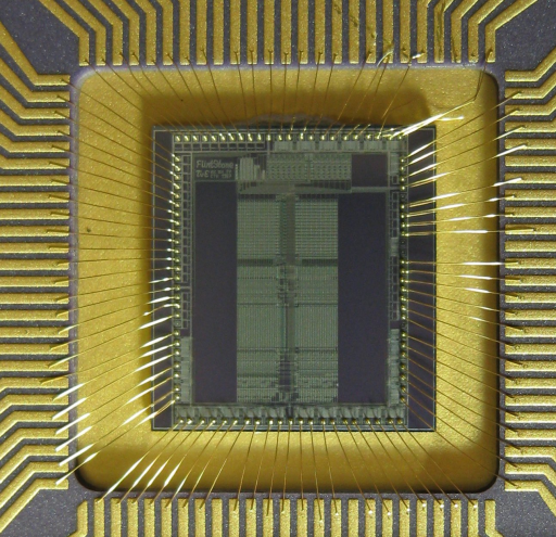
The Flintsone microcontroller is a microprogrammable device designed as a processor for a second version of the Lilith computer. It has some architectural similarities regarding the well known AMD 2901 bit-slice processor, but is fully 32-bit. Some special bit operations are implemented to support graphic applications, and the chip contains a complete address hardware with a 4x14bit microprogram stack. The device, consists of a 16x32 dual read - signle write register bank, an ALU and bit operations unit (FFO- Find First One), a shifter and supporting hardware for multiplication and division.
There is one known bug in the first release of the chip: If the condition of a conditional jump to a subroutine does not hold, the return address (contents of the PC register) is, nevertheles, pushed onto the stack. Therefore, only unconditional jumps should be used for the time being.
The following is an excerpt from Technical Report 117 of the Computer Science department of ETH Zurich from October 1989 by Niklaus Wirth
Flintstone is - in this context - the name of a microprogrammanble microprocessor. It consists, like the common flintstone, of silicon or - to be more precise - of silicon oxyde. This at least since July 1989. Before that date, it existed on paper only, its architecture having been defined by the author in the summer of 1983. At that time, or rather even earlier, the idea existed to design and build a more powerful, more highly integrated version of the Lilith computer. The idea was soon dropped for economic reasons, and teh purpose of Flintstone was rather seen as a fast and felxible coprocessor for rater operations on the one hanbd, and as a processor optimally suited to display the essentials of a processor architecture and to exercise the craft of microprogramming.
Plans to implement Flintstone were picked up bu M. Morf, but they didn't come to fruition and the project seemed buried. In 1985, W. Fichtner, head of the Institute for Integrated Systems at ETH rediscovered Flintstone in serach for projects suitable for gaining design experience for integrated circuits, the design appearing to be neither too simple, nor too complicated for the available tools and technology. Flintstone's layout was designed by Th. von Eicken as a student project, in fact twice because during the design phase the fabrication process and its parameters had been altered. The layout had been completed in the fall of 1987 for Faselec's Sacmos fabrication process with a 2u gate width.
In the summer of 1989, a Flintstone wafer become available and samples were tested by H. Bonnenberg and N. Felber. They reach a clock rate of about 8 MHz. The interest in Flintstone primarily focusses on its use as a vehicle for microprogramming a RISC-type architecture in a laboratory environment. To make available a suitable description of the processor is the primary reason for writing this report. Another is the opportunity to acknowledge the many contributions that have moved Flintstone from paper to silicon and to thank all the participants for their experience and endurance.