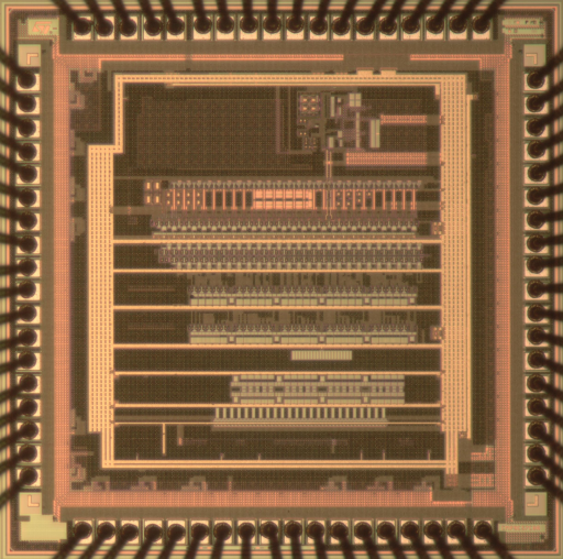
The IIS Chip Gallery
Folding_ADC (2006)

by

| Application | Converter |
| Technology | 130 |
| Manufacturer | STM |
| Type | Reserach Project |
| Package | LCC84 |
| Dimensions | 1500μm x 1500μm |
| Voltage | 1.2 V |
| Power | 195 mW |
Continuous growth in digital communications, multimedia and consumer products requires analog-to-digital converters (ADCs) of 8-10 bits resolution and sampling rates in excess of 100 MHz.
Folding and interpolating ADC inherits speed advantages from flash architecture by maintaining one-step nature, but its resolution is heavily limited by the poor mismatch of differential pairs in CMOS technology. The use of interpolating and averaging improves mismatch performance, but fairly large MOSFET device sizes are still needed to maintain reasonable offsets, which leads to slow speed. To reduce the impact of offset on speed, two preamplifier stages, which employ open-loop auto-zero technique to cancel their own offsets, are inserted before the folding amplifiers. Because of the gain of the preamplifiers, the offset contribution from the folding amplifiers and fine comparators is greatly reduced. Consequently, small devices can be used, which improves the speed-accuracypower trade-off.
The prototype ADC has been implemented in a 130 nm CMOS technology, and occupies 1.8 mm2 active area. It achieves 200 MS/s sampling rate while consuming 195 mW from a 1.2 V supply. The SNDR (signal-to-noiseand- distortion-ratio) reaches 53.5 dB for low frequency inputs, and 51.8 dB for those close to Nyquist frequency.