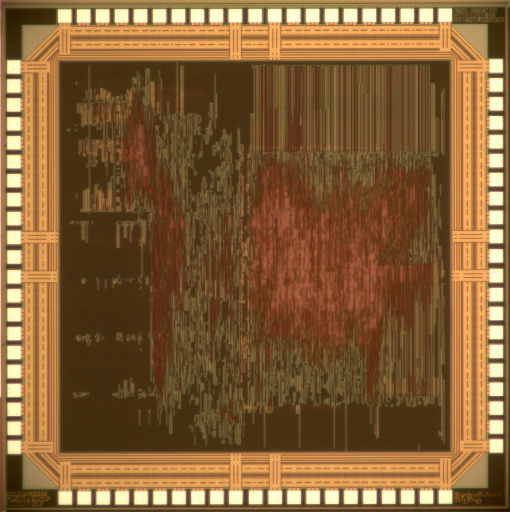
The IIS Chip Gallery
Edge_Receiver (2008)

by

| Application | Communication |
| Technology | 180 |
| Manufacturer | UMC |
| Type | Semester Thesis |
| Package | LCC84 |
| Dimensions | 2500μm x 2500μm |
| Voltage | 1.8 V |
EDGE is an extension to the cellular standard GSM. It was introduced in 1999 and allows up to three times higher data rates than GSM. Due to the introduction of 8-PSK modulation in the GSM/EDGE standard, the channel equalizer used in GSM systems becomes too complex for hardware implementation, hence new equalization strategies are required.
The master thesis of Claudio Foelmli dealt with the design and the hardware implementation of a Turbo Equalizer for the cellular standard EDGE. A simulation environment comprising the baseband transmitter part, the cellular channel and the baseband receiver part has been implemented and applied for simulations. In these simulations, architecture alternatives like different channel decoders, channel estimators and channel equalizers were compared and verified against each other.
A parallel semester thesis dealt with the ASIC implementation of a baseband receiver for the cellular standard EDGE. The simulation results of the master thesis of Claudio Foelmli have been used for finding a fixed-point model, which shows a good trade-off between demodulation performance and hardware complexity.
The channel equalizer in the design uses the concept of linear equalization operating in the frequency domain for reducing the hardware implementation complexity. An efficient realization of this ?frequency domain equalizer? (FDE) has been implemented together with an 8-PSK demodulator. Furthermore, solutions for the burst demapper, de-interleaver and channel decoder have been found, supporting several operating modes as specified for EDGE. A major difficulty in this project was the efficient implementation of flexible design blocks, which enable the receiver to support several operating modes with different transmission block sizes, puncturing rates, and interleaving patterns as specified for EDGE.
With three system clocks running on different frequencies and 15 RAM macro blocks, the backend design has been another complex task in this VLSI semester project. The final ASIC design has been verified and tested on the digital tester of the institute.