The IIS Chip Gallery
Eagle (2009)

by

| Application | Communication |
| Technology | 90 |
| Manufacturer | UMC |
| Type | Diploma Thesis |
| Package | QFN56 |
| Dimensions | 1875μm x 1875μm |
| Gates | 400 kGE |
| Voltage | 1.2 V |
| Power | 250.8 mW |
| Clock | 431 MHz |
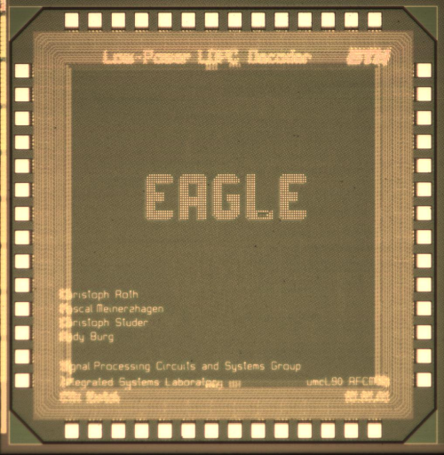
The high throughput and quality-of-service requirements of today's wireless communication systems require highperformance error-correction schemes. Low-density parity- check (LDPC) codes are widely used due to excellent error-correction capabilities. Especially, quasi-cyclic (QC) LDPC codes offer high decoding throughput at relatively low implementation complexity. Mobile applications ask for low-power VLSI implementations of LDPC decoders which do still achieve the high throughputs.
In this project, various low-power strategies ranging from the arithmetic level down to the gate level have been applied to an existing LDPC decoder design: Introduction of an adapted layered offset min-sum (L-OMS) decoding algorithm, replacement of SRAM macrocells by latch arrays, change of number representation format from two's complement to sign-magnitude, and memory bypassing. The initial power consumption and the power consumption after each optimization step have been determined by means of an automated power flow, considering both nominal supply voltage and scaled supply voltages.
With respect to the original design, the total power consumption could be reduced by nearly 72 %. The high achievable throughput of approximately 1.5 Gbit/s allows to extensively use voltage scaling while still fulfilling the throughput requirements. The design supports all QCLDPC standards, the code blocks and matrix prototypes fit which fit into the allocated memories. The decoder has been implemented in 90 nm CMOS technology.