The IIS Chip Gallery
Wirthlinx (1995)

Additional pictures below, click to see larger versions

by


| Application | Processor |
| Technology | 1000 |
| Manufacturer | ES2 |
| Type | Research |
| Package | DIP40 |
| Dimensions | 5500μm x 4800μm |
| Clock | 100 MHz |
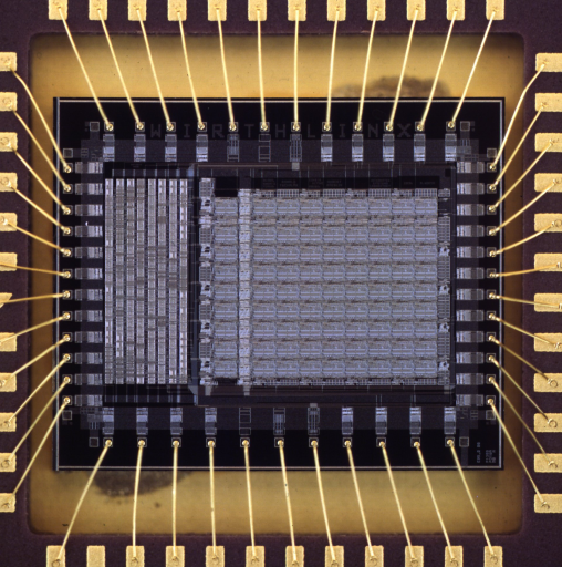
This design is the prototype of an FPGA based on an architectuire suggested by Prof. N. Wirth. It contains 9x9 Configurable Logic Blocks (CLB's). The full FPGA would have 32x32 CLB's grouped into 16 blocks of 8x8. Each CLB is able of perfroming an arbitrary function of two inputs and a limited number of functions of three, with the option if a flip-flop at the output. The resulting structure is very fine-grained. Communication is neighbour to neighbour or via horizontal and vertical busses wchich span a complete block.
Each CLB can be configured separately, enabling fast partial reconfiguration of the FPGA. A separate configuration clock allows for maximum speed of teh configuration process. To hold the configuration a compact, semi-dynamic shift register was developed.
Because of the regularity of and size constraints the CLB's and block-connector cells were all done in hand-layout; only some logic used for controlling the configuration was done in standard cells.
The prototype was successfully tested , revealing only two minor bugs which did not affect normal operation. Maximum configuration speed is 45 MBits/sec; maximum operating frequency is 100 MHz, with a CLB delay of less than 7.5ns.