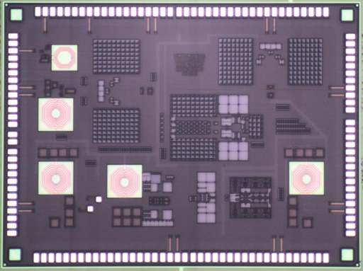
The IIS Chip Gallery
Lemon (2002)

by

| Application | Communication |
| Technology | 130 |
| Manufacturer | Infineon |
| Type | Research Project |
| Voltage | 1.5 V |
| Power | 44.25 mW, 1.5V |
To offer higher data rates to mobile communications users, third generation Universal Mobile Telecommunications System (UMTS) services will become available in the imminent future. For better customer acceptance and full area coverage, multimode terminals including GSM (Global System for Mobile Communications) capabilities in small form factors and with decent standby times are a must.
Baseband Circuits for Direct Conversion UMTS Mobile ReceiverIn this project, a direct-conversion transceiver has been developed, eliminating the need for external, passive filters for image rejection and for channel selection. In the zero-IF receiver, the baseband part is of particular importance, combining accurate gain control and channel select filtering with low noise and high linearity requirements. Additionally, since amplification takes place around DC, offset compensation must be provided.
The baseband filter, like the whole transceiver, has been integrated in a 0.12?m CMOS process. It includes a sixth order leapfrog low pass filter, a first order all pass, an offset compensation loop and an automatic tuning circuit that fixes the filter cut-off frequency under process and temperature variations. Compared to the 0.25um CMOS prototype described in the last research review, the power consumption has been significantly reduced from 37.5mW to 8.25mW, owing partly to the reduction in supply voltage (from 2.5V to 1.5V), but also to the significantly reduced current consumption (from 15mA to 5.5mA). Such a low power design allows longer standby times from a smaller battery, significantly enhancing the mobile terminal.
UMTS Transmit I/Q ModulatorRecently, a first integration for this project has been able to show that direct up-conversion transmitters based on CMOS technology fulfil the high linearity and low power requirements of 3rd generation WCDMA cellular radio networks.
A remaining limitation of the direct up-conversion architecture is carrier leakage. Due to power accuracy and error vector magnitude (EVM) reasons, carrier leakage must be kept low for all gain settings. This makes it difficult to implement a wide range of accurate gain control in the baseband section of a mobile terminal. Circuit techniques to suppress carrier leakage therefore hold the key to a high integration level through the direct up-conversion architecture.
In this contribution, circuit and calibration techniques are investigated that significantly improve carrier leakage. For this purpose, a fully integrated WCDMA Tx IC has been implemented in a 0.12um CMOS process. It includes a baseband filter, an I/Q divider, an I/Q modulator, a variable gain RF pre-amplifier and a carrier leakage calibration loop. The chip has been fully characterized and shows excellent performance at very low power consumption.
LNA and I/Q Demodulator for UMTS ReceiverThe direct conversion architecture is a very attractive candidate for highly integrated UMTS receivers. It avoids the image suppression problem and allows higher integration by reduction of the bulky external components at the price of tougher building block specifications.
The I/Q demodulator design for a homodyne receiver is a challenging task, which requires thorough circuit understanding and very careful design. For the second version of the I/Q demodulator, in order to overcome the limitations of the reduced voltage headroom, a new improved architecture has been chosen. The I/Q demodulator has been fabricated in a 0.12\u03bcm CMOS advanced technology and has been evaluated successfully. A voltage gain of 12dB, an equivalent input referred noise voltage of 4.8nV/sqrt(Hz), an iIP3 of 0dBVrms and an iCP which equals -18.7dBVrms have been measured. The I/Q demodulator consumes 6mA of current.
As a part of the receiver a single-ended low-noise amplifier (LNA) with matched input and output to 50Ohm has been designed, implemented in a 0.12um CMOS technology and successfully tested. Power gain of 12dB, noise figure (NF) of 2.3dB, iIP3 of 5.4dBm and iCP of -12dBm have been measured. The LNA draws a current of 6.5mA.
Carrier-Leakage Suppression in Direct-Conversion WCDMA TransmittersModern communications standards like 3GPP UMTS (WCDMA) pose very stringent requirements on mobile transmitters. Large output power control range combined with high linearity and low power consumption make the design of a direct up-conversion (DUC) transmitter a very demanding task.
This research work solves the problem of the carrier leaking to the signal band. In the direct up-conversion architecture this component is in the middle of the channel and degrades the quality of the modulated signal. Three different techniques can be applied, each by itself or together in order to suppress the carrier leakage. Firstly, some or all of the gain control can be done in the RF part of the transmitter. Secondly, at lower gain settings the bias current in the modulator can be reduced. Finally, calibration can be used if the previously mentioned techniques are not able to fulfil a given specification. Calibration relies on the fact that mismatches in the baseband circuit and the modulator bias current sources lead to a DC offset that appears as carrier leakage. The baseband circuits and the modulator have been extended so that it is possible to control the amount of carrier leakage. The carrier leakage is detected with a simple RF power detector. Its output is used by a digital calibration algorithm that sets the transmitter?s carrier control inputs in order to minimize the amount of carrier power at the output.
Measurements have shown that the applied carrier suppression techniques work very well and enable the DUC architecture to be used even for very demanding communication standards.