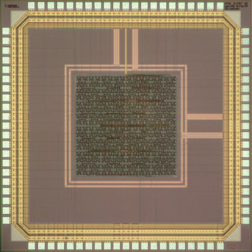
The IIS Chip Gallery
Adiabatic (2004)

by

| Application | Low-power |
| Technology | 250 |
| Manufacturer | UMC |
| Type | Research Project |
| Package | LCC84 |
| Dimensions | 2500μm x 2500μm |
| Gates | 30 kGE |
| Voltage | 2.5 V |
| Power | 0.045 mW, 0.8V, 0.67MHz |
| Clock | 0.67 MHz |
The fundamental cause of CMOS dynamic power dissipation is the organization of the energy transport in the circuit. Charging and discharging an internal node capacitance requires an energy injection from the driver proportional to the load and to the square of the supply voltage. Hence, to decrease the dissipation in standard CMOS circuits, the designer must minimize the switching events, reduce the node capacitance, decrease the voltage excursion, or apply some kind of combination of these methods. The problem is particularly critical inside the clock network of the design, where up to 40% of the total energy are dissipated.
Yet, when timing is not a major issue, resonant clocking can represent an efficient alternative to standard clocking. This technique allows the recycling of the energy from the large capacitance of the clock net, which is put in resonance with a small external inductance.
In the frame of this project, a high-order general-purpose FIR filter for low-rate audio application with a fully resonant clocking strategy has been designed. Among the features of this 110k-transistors design, probably the largest ever realized with such a clocking strategy, are: