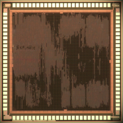
The IIS Chip Gallery
Multimode_DFE (2005)

by

| Application | Communication |
| Technology | 130 |
| Manufacturer | STM |
| Type | Research |
| Package | PGA100 |
| Dimensions | 2270μm x 2270μm |
| Voltage | 1.2 V |
| Power | 47.52 mW, 0.9V, 122.88MHz |
| Clock | 26-220 MHz |
Low power consumption, small area, high integration grade, programmability, portability, versatility, high speed and yield, low production and assembly costs can not be met all at once on a single die: industry has to find a trade off among those criteria, to face the extremely high concurrence in the growing world of telecommunications.
While programmable architectures guarantee high flexibility in a wide range of applications, custom implementations assure smaller area occupation and lower power consumption. While programmable architectures need very advanced technologies to assure a certain throughput, custom implementations reach the target performance by using technologies which still welcome easy analog circuitry on-chip and benefit of high yield. The aim of the present project is to compare an optimal custom design solution in terms of power and area savings with more flexible approaches such as FPGAs or DSPs.
A digital front-end for GSM/WLAN/WCDMA wireless communication standards has been implemented, together with 3G UMTS base-band signal processing. Particular care has been dedicated to lower the power consumption: massive clock gating has been introduced into the architecture, to minimize the switching activity. Temporarily unused blocks are powered down. Low-Vt cells have been replaced by high-Vt cells where timing closure was not critical: these measures reduced the core leakage power down to less than 1 mW. The overall core power consumption is excellent with only 50 mW @ 120MHz showing that a dedicated hardware solution is still very attractive for mass market applications.