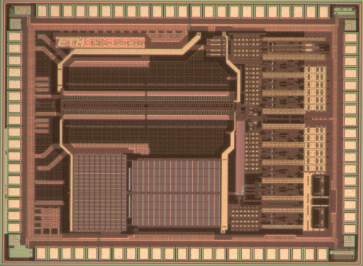
The IIS Chip Gallery
Armadillo (2010)

Additional pictures below, click to see larger versions

by


| Application | Converter |
| Technology | 130 |
| Manufacturer | STM |
| Type | Research |
| Package | CQFP84 |
| Dimensions | 2350μm x 1850μm |
| Voltage | 1.2 V |
| Power | 100 mW |
| Clock | 200 MHz |
As well as being important in its own right, the digital-to analog converter (DAC) is an increasingly used building- block in modern electronic systems ranging from advanced communication devices to high-performance analog-to-digital converters. The design of such DACs in a standard sub-micron CMOS technology using a lowsupply voltage remains a challenging task. The majority of DAC architectures in deployment today are predominantly one of two types: current-steering or switched-capacitor. The current steering architecture consists of an array of current sources that are switched to the output node. Due to the inherently fast speed at which these currents can be switched, this topology is favourable in high-speed applications such as modern communication systems. Switched-capacitor DAC topologies rely on charge redistribution and are realised using a network of switches and capacitors. Although they cannot reach the high-speeds attained by current-steering designs, they have the advantage of delivering good linearity and accuracy. Hence they find widespread use in sampled-data systems requiring a DAC such as SD-modulators, pipeline and successive approximation ADC architectures.
This research project has culminated in the development of a high-resolution hybrid DAC. The DAC targets a resolution of 15 bits by merging a calibrated 6 bit switched capacitor MSB sub-DAC with a 9 bit current-steering LSB array. The reference current for the LSB array is generated on-chip using dedicated circuitry in conjunction with one of the MSBs from the switched-capacitor sub-DAC. A general-purpose 0.13 mm CMOS technology featuring MIM capacitor option is used in the implementation of the chip. The DAC is designed to run at a sampling frequency of 200 MHz and operate from a mere 1.2 V supply voltage.