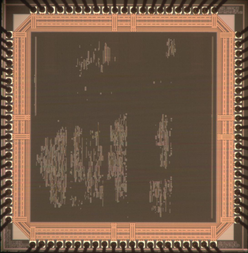
The IIS Chip Gallery
SVD_Devaanoom (2007)

by

| Application | Communication |
| Technology | 180 |
| Manufacturer | UMC |
| Type | Semester Thesis |
| Package | LCC84 |
| Dimensions | 2500μm x 2500μm |
| Voltage | 1.8 V |
| Power | 160 mW (SVD) |
This chip is shared by two designs:
Singular Value Decomposition for MIMO Systems
The singular value decomposition (SVD) and the QR decomposition (QRD) are two of the most prominent matrix decomposition algorithms. Both algorithms are used in various signal processing applications. In the field of wireless multiple-input multiple-output (MIMO) communication systems, the SVD and the QRD are employed for eigenmode transmission (beamforming) and for channel matrix preprocessing respectively.,?p>
In this project, two minimum area matrix decomposition units (MDUs) have been designed. Both units are programmable to perform QRD and SVD with variable arithmetic precision. The QRD algorithm uses Givens rotations that are efficiently computed by a CORDIC. For the SVD, the well-known algorithm of Golub et al. has been used, which only requires an additional multiply-accumulate (MAC) unit.
Two MDUs have been implemented: one unit has been optimized for throughput (i.e., MDU I), whereas the throughput of the MDU II is tunable at run time by reducing the arithmetic precision. The ASIC is able to decompose complex-valued 4x4-dimensional channel matrices and has been implemented in 0.18 mm CMOS technology. The VLSI implementation achieves a hardware efficiency of up to 325 k SVD/s/mm2 and 1.92 M QRD/s/mm2. The power consumption is between 105 mW and 155 mW for the QRD and 106 mW and 160 mW for the SVD respectively
High-Throughput Cryptographic Core with Authentication
This master thesis presents a design-space exploration of the Galois/Counter Mode (GCM) algorithm with Advanced Encryption Standard (AES) as underlying block cipher for high-throughput applications to combine data encryption and message authentication. Emphasis was put on finding suitable hardware architectures for a cryptographic core using reasonable hardware resources for the desired throughput rates. Regarding the AES algorithm, different SubBytes and round architectures were evaluated against each other. Using composite field algebra, the area requirement for the SubBytes operation decreased by 36 % compared to implementations based on lookup tables. For the multiplier required for GCM, two bit-parallel, a digit-serial and a hybrid architecture were investigated. The different architectures were designed, implemented and tested on a Xilinx Virtex4-FX100 FPGA. All architectures support key lengths of 128, 192 and 256 bits and are equipped with a ready-to-use interface for real-world applications. For the GCM-AES cryptographic cores throughput rates from 1.8 to 26.2 Gb/s were reached.
Backend designs of the ASIC design flow were performed for various architectures in order to also show the capabilities of ASIC implementations. Finally, one of the architectures was implemented on an ASIC using a 0.18um CMOS process.
Collaboration with IAIK - TU Graz