The IIS Chip Gallery
Pipelined_Adder (1994)

by

| Application | Processor |
| Technology | 1000 |
| Manufacturer | Faselec |
| Type | Research Project |
| Package | DIP40 |
| Dimensions | 2000μm x 3300μm |
| Gates | 3 kGE |
| Voltage | 5 V |
| Power | 775 mW (800 MHz, 5V) |
| Clock | 800 MHz |
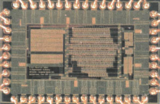
An 8-bit adder has been implemented with the 1.0um self aligned CMOS process of Faselec AG and successfully tested up to 800 MHz at a power consumption of 755 mW at 5V supply voltage. At 3V supply voltage the maximum operation frequency is 480 MHz, and the current 48mW. A single-stage bit-serial adder has also been implemented in the same technology and tested to be functional at more than 1 GHz, consuming only 60mW. The 8-bit adder chip performs addition of two 8-bit data words and has a carry input provided for subtractions. The data throughput of 800 million additions per second is achieved with a dedicated architecture, fine-grain pipelining, merging the combinational logic into pipeline registers, and by careful transistor sizing.
The architecture of the 8-bit adder is based on carry increment adders. The scheme is siilar to carry-select adders but instead of selecting between two results, the carry input increments or passes the intermediate result. The area compared to a standard carry select architecture is thereby reduced by about one third.
New logic flip-flopd, based on our fast dynamic flip-flops for prescalers, have been developed. Compared to a standard pipeline, where the combinational logic is always located between the register stages, these gates have been merged into registers. Thereby the propagation delay of the combinational gate is shared with the delays of the flip-flop, significantly reducing the cycle time of a pipeline stage.