The IIS Chip Gallery
GSM_filter (1997)

by

| Application | Communication |
| Technology | 250 |
| Manufacturer | Toshiba |
| Type | Research |
| Package | Baredie |
| Voltage | 2.5 V |
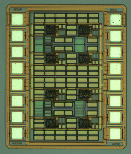
In this work all the critical building blocks required for a 900 MHz GSM transceiver (except the frequency synthesizer) have been designed using a 0.25um CMOS technology. The receiver part comprises a low-noise amplifier (LNA), a double-balanced mixer (DBM) and a complete IF strip. The transmitter part comprises a TX modulator and a TX preamplifier.
The LNA has 16 dB gain and a 1.85 dB noise figure. It provides 50Ohm impedance at both input and output using only one external inductor, and consumes 10.8 mA. The DBM provides 8.5 mS conversion gain, a 12.6 dB SSB noise figure and 8.8 dBm IP3. It draws 6 mA from the 2.5 V supply. The 71 MHz IF-amplifier has a programmable gain from -20 to 60 dB in 2 dB steps. The quadrature demodulator is implemented using double-balanced mixers for local oscillation rejection and a digital divide-by-2 phase shifter; the demodulator is followed by 150 kHz 4-th order Bessel filters. The complete IF strip consumes less then 5 mA. The quadrature modulator is implemented with double- balanced mixers and a phase shifter. The TX preamplifier has a gain of 20.9 dB and an output compression point of 5.8 dBm. The TX parts consume less than 50 mA which is negligible in comparison to the current needed by the power amplifier.
There are several small blocks involved in this project:
See also the final project GSM.