The IIS Chip Gallery
JPEG_Bahnsignal (2005)

by

| Application | Graphics |
| Technology | 250 |
| Manufacturer | UMC |
| Type | Semester Thesis |
| Package | LCC84 |
| Dimensions | 2500μm x 2500μm |
| Gates | 25 kGE |
| Voltage | 2.5 V |
| Clock | 80 MHz (JPEG) MHz |
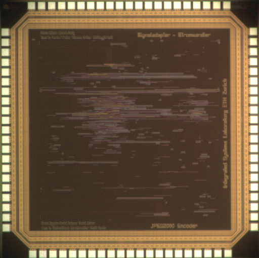
This chip contains two completely unrelated designs:
JPEG2000 Encoder VLSI ImplementationtJPEG2000 was announced as successor of the well known JPEG standard. It is a new image coding system that relies on wavelet transformations. Some of its major enhancements with respect to JPEG include: capability of lossy and lossless compression, higher error resilience, region of interest (ROI) coding, and improved performance at low bit rates. For encoding, a discrete wavelet transform (DWT) is first applied to the input image, leading to wavelet coefficients. These are quantized and entropy- coded before forming the output bitstream, using a so called EBCOT scheme.
In this project, a ASIC implementation of a JPEG2000 encoder has been developed. The three main system building blocks (lifting based DWT, context formation, arithmetic coder) which perform the entropy coding by the EBCOT scheme are enabled by a main controller responsible for the correct chaining of the encoding steps. The access of the three blocks to the external memory necessary to cope with the demanding storage requirements of the standard is also handled by the main controller.
The implemented encoder occupies an area of 1.2mm2 on a 0.25 um 1P/5M CMOS process. It runs at a clock frequency of 80 MHz which permits to achieve an encoding rate of 3.6 Mpixel/s.
ASIC for Railway Signal MonitoringThe safe operation of railway signals is mandatory also for older signals which have no electronic supervision implemented. Siemens provides an adapter which allows to connect such signals to standard monitoring systems.
The existing system supervises the state of the incandescent lamps and provides this information through a serial data interface to the monitoring system.
The goal of this semester project was to re-design a PCB board by moving as much of the analog signal processing into the digital domain and to combine all digital functionality in an FPGA. The new realization saves space and cost, and enhances security.
The implemented circuit controls several current-to-digital converters, filters the sampled signals, detects the state of the lamps (on, off, blinking), composes the electronic telegram and sends it over the serial port. A sophisticated failure control system is included and its response is transmitted together with the lamp state information.
In order to learn ASIC design from specification to test, the students implemented the digital system in an ASIC which was successfully tested during the VLSI course.
The circuit implemented in 0.25um 5 metal-layer CMOS technology covers 0.5 mm2 area and contains some 100,000 transistors.