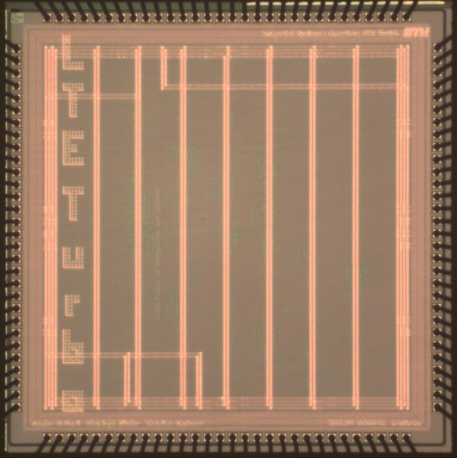
The IIS Chip Gallery
LTEturbo (2009)

Additional pictures below, click to see larger versions

by


| Application | Communication |
| Technology | 130 |
| Manufacturer | UMC |
| Type | Research Project |
| Package | PGA120 |
| Dimensions | 3240μm x 3240μm |
| Gates | 700 kGE |
| Voltage | 1.2 V |
| Power | 70 mW, 80MHz |
| Clock | 302 MHz |
Recent popularity of smart phones, netbooks, and other mobile broadband devices has vindicated 3G (HSDPA) as an enabling technology for main-stream high-speed data and has given fresh impetus to its 4G successor LTE (long-term evolution). LTE achieves up to 326.4 Mb/s throughput, which leads to more than 20 times higher complexity for turbo decoding (compared to HSDPA).
In this project, a low-power turbo decoder implementation for LTE, which is able to achieve the LTE peak throughput, has been developed. To this end, we designed a highperformance contention-free interleaver architecture, which contains two Batcher sorting networks to perform 8-fold parallel interleaving, i.e., the architecture enables interleaved memory access to eight log-likelihood ratio (LLR) values per clock cycle. By instantiating eight parallel radix-4 maximum a-posteriori (MAP) decoder cores, the LTE peak throughput could be achieved.
Measurement results of the fabricated chip show that the 130 nm CMOS ASIC achieves a maximum clock frequency of 302 MHz, ultimately leading to peak throughput of 390.6 Mb/s at 5.5 iterations. The theoretical LTE maximum throughput can therefore be achieved with margin. At more realistic 100 Mb/s throughout, the measured power consumption is only 68.6 mW, which is comparable to that of state-of-the-art low-power turbo decoders for HSDPA that achieve one magnitude lower throughput.
Sandro actually worked on the MBCJR Decoder during his semester thesis. He continued working on this chip almost without an interruption. Eventually he started his Ph.D. at IIS as well.
This chip was finished while Christoph Studer was enjoying his honeymoon, there is a small message to commemorate this on the chip.