The IIS Chip Gallery
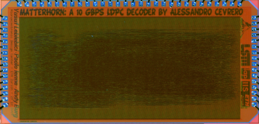
Matterhorn (2009)

Additional pictures below, click to see larger versions


by


| Application | Communication |
| Technology | 90 |
| Manufacturer | UMC |
| Type | Research Project |
| Package | PGA120 |
| Dimensions | 3950μm x 1875μm |
| Gates | 1400 kGE |
| Voltage | 1.2 V |
| Power | 1'606.7 mW |
| Clock | 136.90 MHz |
Low density parity check (LDPC) codes are very powerful forward-error-correcting codes that enable digital communication systems to operate extremely close to the Shannon Limit. The basic idea of these codes and a possible approach for the decoding was discovered as early as in the 1960s by Gallager. Unfortunately, at that time, the decoding process was considered to be too complex for implementation, and the codes received only very little attention. With the advent of very large scale integration, LDPC codes were rediscovered in the 1990s, and the parallel nature of the message passing algorithms used for decoding turned out to be well suited for deep-submicron integration of decoders for high-speed applications.
In this work, we consider the problem of realizing LDPC decoders for optical networking appliances with a throughput above 10 Gbps. In this first project, an LDPC decoder for 10 Gbps Ethernet was realized in a 90 nm process together with the Microelectronic Systems Laboratory of the EPFL. The various challenges in this project relate to the selection of the decoding algorithm, to the choice of the fixed-point implementation parameters, the design of the register-transfer-level implementation, and especially to the physical implementation. The main problem driving most of the design decisions was the fact that the usual parallel LDPC implementations would occupy a prohibitive active silicon area and would suffer from a very poor area utilization due to the significant amount of routing that is required to connect thousands of mostly identical building blocks.
This challenge was met by employing a layered decoding strategy, combined with an innovative interconnect architecture that reduces the amount of wiring significantly to enable an area utilization above 90% for the final design and to provide a throughput above 10 Gbps.
This chip is joint work with the Microelectronic Systems Laboratory of the EPFL Lausanne.