The IIS Chip Gallery
Bogazici (2010)

Additional pictures below, click to see larger versions

by


| Application | Test |
| Technology | 90 |
| Manufacturer | UMC |
| Type | Research |
| Package | QFN56 |
| Dimensions | 1875μm x 1875μm |
| Gates | 90 kGE |
| Voltage | 1.2 V |
| Power | 1 mW |
| Clock | 1 MHz |
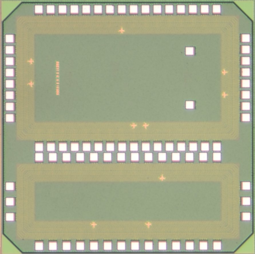
This is a test chip containing two independent blocks. The upper block contains different logic-compatible multilevel gain-cell-based DRAM designs, while the lower block contains several implementations of a cubehash function based on different dynamic flip-flop topologies. Each block has several power domains and requires special power pads, marked with a cross (cf. Picture above), which are not connected to the default power domain.
The chip name Bogazici continues a series started with the previous chip from Pascal named Unidad by using famous bridges as the name. In this case, a Turkish bridge was used as one of the designers, Onur, comes from Turkey.
Among the major options for on-chip memory integration, namely dynamic random access memory (DRAM) and static random access memory (SRAM) macrocells, DRAM typically uses special technology options to build high-density stacked or trench capacitors and is therefore not logic compatible, while SRAM is compatible with standard logic CMOS technologies but has, with a minimum of 6 transistors per cell, a relatively large cell size.
In gain cells, charge is stored on the gate of a transistor, whose transconductance gain is used to yield a high sensing current, which leads to a fast and non-destructive read-out operation. Furthermore, gain-cell-based DRAMs can be logic-compatible and smaller than SRAM. Various gain-cell-based DRAMs have been proposed to date.
In order to trade data retention time for per-area storage density, many bits can be stored in a single dynamic cell. Various multilevel DRAMs using a conventional 1T-1C storage cell have been proposed to date.
In this project, the multilevel approach is applied to gain cells for the first time in order to yield a high-density logic-compatible storage element. To sense different levels, the drain current of the storage transistor is modulated by means of its gate voltage.
For the design of digital signal processing systems, with applications ranging from wireless communications to cryptography, we did so for relay on standard cells in general and flip-flops (FFs) in particular provided by a standard cell library provider. Among a large variety of FF classes and topologies, most library providers offer only static transmission-gate-based master-slave FFs. Even though this FF topology exhibits high reliability under large process-voltage-temperature (PVT) variations and might qualify as a good general FF topology for a broad range of applications, it is surely not optimal in terms of delay, area, and power consumption.
Recent publications report on exhaustive FF topology comparisons and allow for finding the best FF topology for each target application, be it high-performance, low-power, or some other applications. However, all FF comparisons reported to date consider only basic FFs, even though most practical systems require FFs which support clock gating, scan chain insertion, and can be (re)set.
In this project, dynamic flip-flops with a scan port and a reset feature have been designed and characterized for the integration in a standard digital design flow. To qualify for a later employment in larger systems, the dynamic flip-flops have first been integrated in a relatively small system, namely a VLSI implementation of a cubehash function.