The IIS Chip Gallery
TwoPhase (2004)

by

| Application | Low-power |
| Technology | 250 |
| Manufacturer | UMC |
| Type | Research Project |
| Package | LCC84 |
| Dimensions | 2500μm x 2500μm |
| Voltage | 2.5 V |
| Power | 2 mW , 0.44mW, 0.56mW |
| Clock | 2 MHz |
Energy efficiency is of primary importance in CMOS circuits intended for the portable market. Replacing the widely used one-phase single-edge-triggered (SET) clocking strategy by a two-phase level-sensitive counterpart in low-frequency applications (e.g. low-rate audio processing, as in hearing aids) makes it possible to do without strong and, hence, energy-consuming clock buffers. While this seems an attractive option, there are trade-offs and limitations.
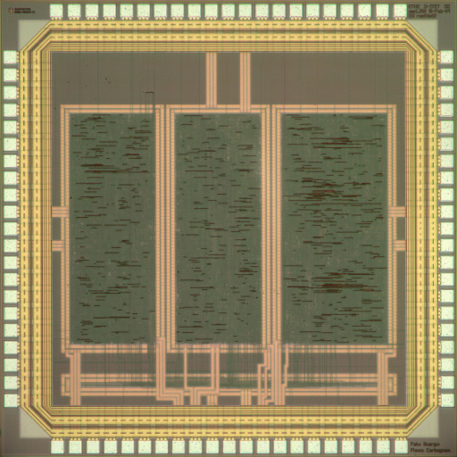
To study the impact of the clocking strategy on the overall power dissipation, three versions of the same high-order general-purpose FIR filter have been designed and merged on the same die (see figure):
The results of the measurements point out that [3] dissipates around 5 times more than the others, demonstrating the energy efficiency of the clock gating technique. Design [1] represents the state-of-the-art of low-power, fully exploiting traditional low-power strategies, such as scaled supply voltage, clock gating and latch-based memories. Two-phase clocking enables a 20% energy savings of [2] compared to the one-phase design [1]. Yet, this energy efficiency is limited by the supply voltage.