The IIS Chip Gallery
Rosetta (2019)

Additional pictures below, click to see larger versions


by


| Application | Pulp |
| Technology | 65 |
| Manufacturer | TSMC |
| Type | Research |
| Package | QFN64 |
| Dimensions | 4100μm x 3000μm |
| Gates | 6 MGE |
| Voltage | 1.2 V |
| Power | tbd mW |
| Clock | 190 MHz |
Rosetta is a PULPissimo based architecture which uses the RI5CY core with the newest vector processing ISA extension and several accelerators for various kinds of signal processing applications. In addition to the Integrated Circuits Laboratory, the chip contains contributions from the Embedded Systems Laboratory and Telecommunication Circuits Laboratory of EPFL our sister university from Lausanne.
The chip incorporates a plethora of different memory technologies. For normal computations with high demands in terms of memory capacity, there are 4 conventional SRAM banks for a total of 512 KiB in size. These four memory banks use an interleaved address space mapping and are accessible by the core as well as the various accelerators and peripherals. Two additional xSRAM banks with a total of 64 KiB that are private to the core are available for simultaneous program execution without bank conflicts. Furthermore, the chip contains a 4 KiB two-port latch based standard cell memory that allows for the execution of small programs at low supply voltages.
Rosetta also contains 64 KiB (in 16 memory cuts) of Gain-Cell eDRAM developed by Telecommunication Circuits Laboratory (TCL), based on conventional logic design rules, which can offer higher density than SRAM. The eDRAM in this implementation has a built-in refresh support and a new option to ease folding of the memory. By adjusting the refresh period, it allows to also explore approximate-computing concepts.
Finally, the SoC incorborates a 32KiB in-sram computing architecture and an innovative memory controller enabling in-situ bitwise operations, addition and multiplications developed by Embedded Systems Laboratory (ESL). These features will be used to accelerate data-intensive applications running on the PULPissimo platform. Associated publications with the in-sram computing by ESL:
On the signal processing side Rosetta contains a programmable autonomous accelerator for Hyper-Dimensional Computing Algorithms with binary-spatter-code based Hypervectors of a dimensionality of up to 2048 bits. The accelerator can either use the SCM memory or the eDRAM as its memory backend to operate with up to 16 prototype vectors. This setup will allow to conduct a side by side comparison of the two different memory technology in terms of energy efficiency for approximate computing, i.e., the SCM operating at low voltages or the eDRAM operating with long refresh periods.
Like most PULP chips, the SoC is rounded off with the availability of a plethora of peripherals like QSPI, I2C, I2S, Camera Interface, UART and last but not least a JTAG-based RISC-V debug specification compliant debug unit with full access to the main memory bus of the system. The whole system is designed to operate at maximum frequency of 190MHz for the RI5CY core, memories and the accelerators and a peripheral clock frequency of 50 MHz using two configurable internal FLLs.
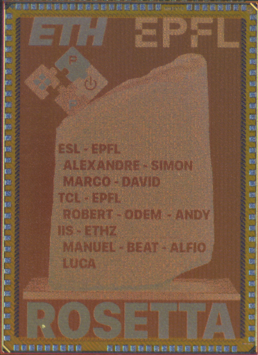
The name of the chip comes from the Rosetta stone the famous stele currently on display in the British Museum that was instrumental in deciphering ancient Egyptian hieroglyphs. It contains the same script in three alphabets which helped scientists to understand the forgotten script of hieroglyphs. There are three separate groups that have contributed to the chip, and one of the implementations of the high dimensional computing for which there is an accelerator is actually language recognition. The logo depicts the outline of the stone in its present shape.
This chip was manufactured by the generous support of the HiSilicon Sponsorship program through the Europractice IC service.